


Figure 2. Macroporous and flexible nanowire nanoES.
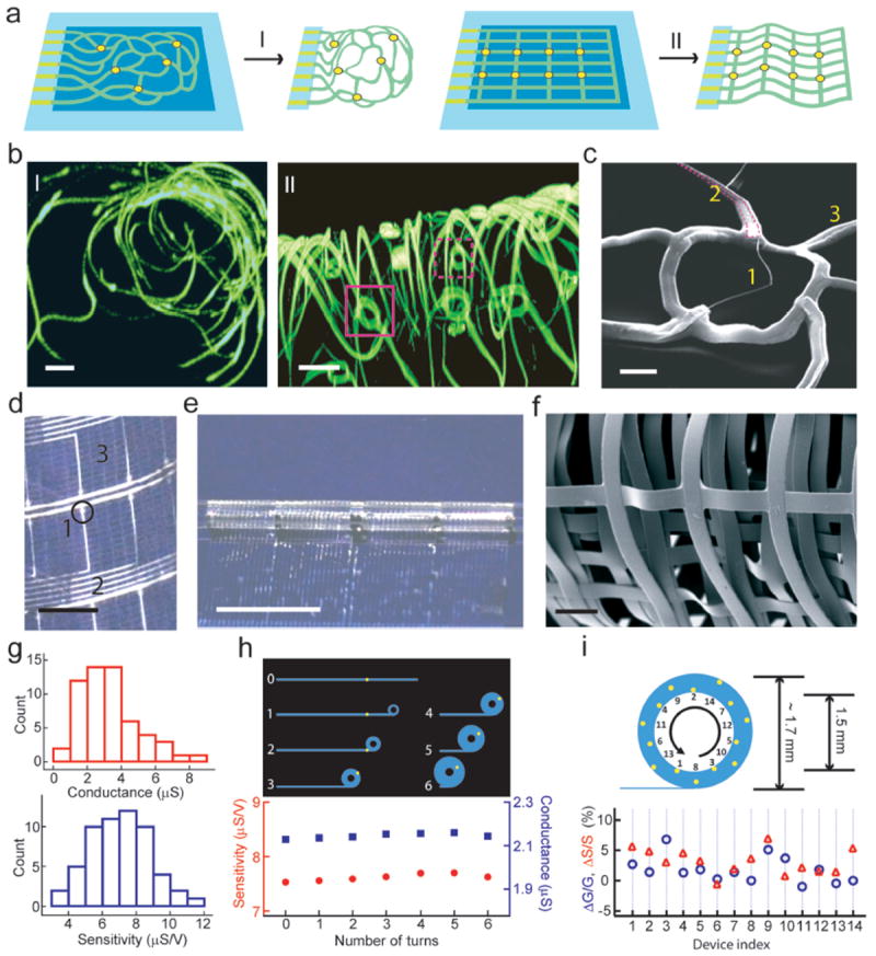
a, Device fabrication schematics. I: Reticular nanowire FET devices. II: mesh nanowire FET devices. Light blue: silicon oxide substrates, blue: nickel sacrificial layers, green: nanoES, yellow dots: individual nanowire FETs. b, 3D reconstructed confocal fluorescence images of reticular nanoES viewed along y (I) and x (II) axes. The scaffold was labeled with rhodamine 6G. The overall size of the structure, x-y-z = 300-400-200 μm. Solid and dashed open magenta boxes indicate two nanowire FET devices located on different planes along x axis. Scale bars, 20 μm. c, SEM image of a single kinked nanowire FET within a reticular scaffold, showing (1) kinked nanowires, (2) metallic interconnects (magenta lines) (3) the SU-8 backbone. Scale bar, 2 μm. d, Photograph of a mesh device, showing (1) nanowires, (2) metal interconnects, (3) SU-8 structural elements. The circle indicates the position of a single nanowire FET. Scale bar, 2 mm. e, Photograph of a partially rolled-up mesh device. Scale bar, 5 mm. f, SEM image of a loosely packed mesh nanoES, showing the macroporous structure. Scale bar, 100 μm. g, Histograms of nanowire FET conductance and sensitivity in one typical mesh nanoES. The conductance and sensitivity were measured in water-gate configuration without rolling. The device yield for this mesh nanoES is 95 %. h, Water-gate sensitivity and conductance of a nanowire FET device during the rolling process in a mesh device. Upper panel, schematic of nanowire FET position (yellow dot) during rolling process; 0-6 denote the number of turns. i, Relative change in conductance and sensitivity of 14 nanowire FETs evenly distributed throughout a fully rolled-up mesh device. Upper panel, schematic of NFWET position (yellow dots). In (h) and (i) the thicknesses of the tubular structures have been exaggerated for schematic clarity.